

")
Tsumoru Shintake, a professor at the Okinawa Institute of Science and Technology (OIST), has created a new, simpler EUV lithography tool that is more affordable than ASML’s versions. If it enters mass production, it could transform the chipmaking equipment market and even the semiconductor industry as a whole.
This new system operates with just two mirrors in its optical projection, a significant change from the traditional six-mirror setup. The main challenge is aligning the mirrors in a straight line, which is vital for maintaining high optical performance and reducing distortions from EUV light. The new optical path enables over 10% of the initial EUV energy to reach the wafer, a considerable increase from the roughly 1% in standard configurations, representing a major breakthrough.

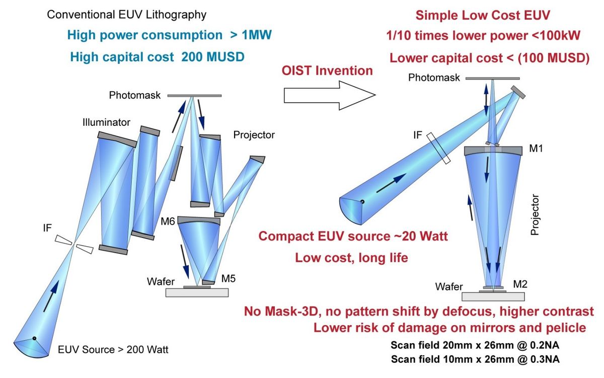
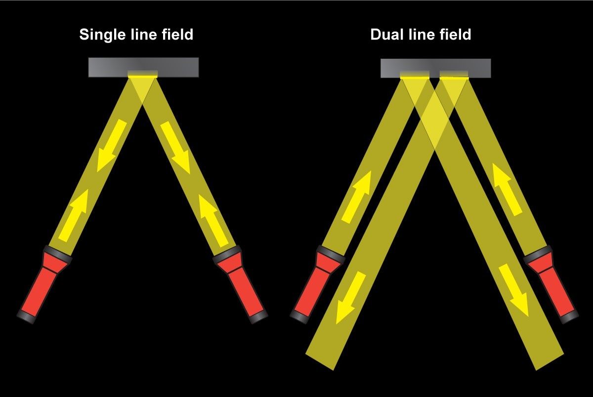
The team led by Professor Shintake has successfully addressed two critical issues in EUV lithography: the prevention of optical aberrations and the enhancement of light transfer efficiency. OIST’s unique ‘dual-line field’ approach allows for photomask illumination without disrupting the optical path, which significantly reduces distortions and boosts image clarity on the silicon wafer.

The capabilities of this innovative system have undergone thorough validation through optical simulation software, demonstrating its proficiency in manufacturing advanced semiconductors. The promising technology has prompted OIST to file for a patent, signaling its preparedness for commercial use. OIST is focused on refining its EUV tool design to achieve real-world applications. The institute believes that this innovation is essential for tackling worldwide challenges, such as the high costs of chip production and the energy demands of semiconductor fabs, which pose risks to the environment.
This invention has positive economic potential. The global EUV lithography market is projected to increase from $8.9 billion in 2024 to $17.4 billion by 2030. With the new, simpler design of EUV tools, more companies may start using EUV systems soon. Still, it is uncertain how near OIST is to bringing its tool to market.


